Laboratories
Department of Precision Engineering
Functional Materials Area
| Assoc. Prof. | Hiroaki Kakiuchi |
| Assoc. Prof. | Hiromasa Ohmi |
For the progress of advanced technology and basic science, it is indispensable to improve the performance of functional materi-als, and also to create materials with new functions. The aims of our researches are 1) to develop new Earth-conscious technol-ogies for the formation of high-quality functional thin films, 2) to create new functional materials, the surface, interface and bulk properties of which are controlled at atomic level, and 3) to fabri-cate highly-functional thin films and to apply them to actual elec-tronic devices. At present, by using atmospheric-pressure, very high-frequency (VHF) plasma, we focus on developing high-rate, low-temperature and ecoclean film growth technologies and also on studying their applications to the production of solar cells, thin film transistors, thin film sensors, and new functional devices.
Nano Surface and Interface Engineering Area
| Prof. | Kenta Arima |
| Assis. Prof. | Kouji Inagaki |
Since the dawn of history, civilization has evolved with persistent efforts to develop manufacturing technologies. In this research area, we are creating novel innovative manufacturing technologies to manufacture state-of-the-art optical elements, semiconductor substrates and MEMS · NEMS devices that require nano- and sub-nanometer order accuracy. Under the philosophy that new technology created by us triggers a new industrial revolution in the 21st century and contributes to the further development of mankind, we are immersed in the research and development of “nanoManufacturing process” that having both extreme precision and efficiency.
Quantum Measurement and Instrumentation Area
| Prof. | Hirotsugu Ogi |
| Assis. Prof. | Yasushi Oshikane |
| Assis. Prof. | Akira Nagakubo |
| Assis. Prof. | Kichitaro Nakajima |
Using our original optical-acoustical measurement systems, we study mechanical behavior of nanomaterials and kinetics of biomolecules, and develop instruments for diagnosis and drug discovery. One important keyword is “resonance”. At resonance, information on mechanical and electromagnetical properties are highly enhanced, allowing high-sensitive measurements in material-biological science. We control sound via light and vice versa to investigate thermodynamic properties in nanofilms, nanowires, and nanodots, and binding and aggregation reactions among various biomolecules. We also study application of our original phonon-photon measurements for biosensors and diagnosis for neurodegenerative diseases, including Alzheimer's disease.
Atomically Controlled Processes Area
| Prof. | Yuji Kuwahara |
| Assoc. Prof. | Akira Saito |
| Assis. Prof. | Takuma Hattori |
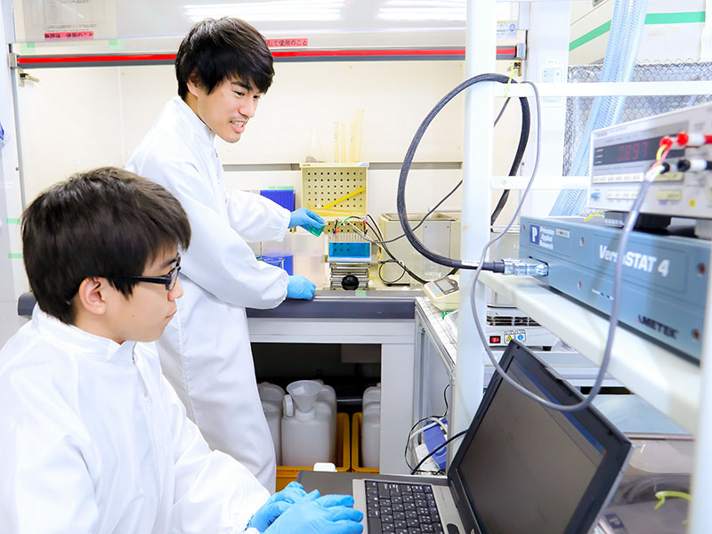
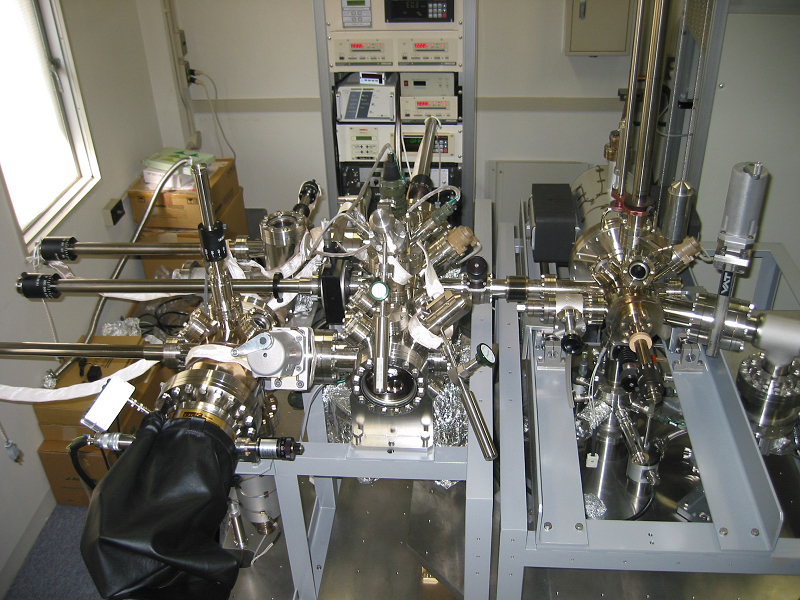
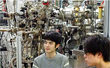
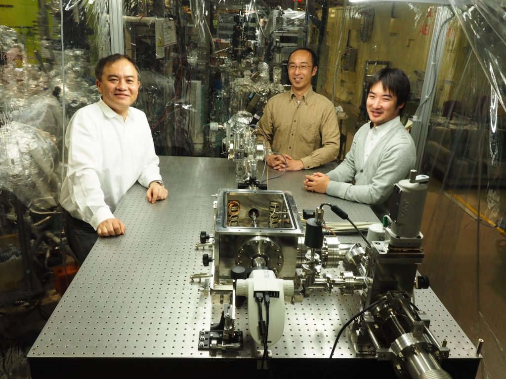
It has become possible to actually view, touch, and move atoms and molecules in the nanometer world, thanks to advances in science and technology. Today we can assemble atoms and molecules to construct synthetic nanometric structures, which do not exist in nature. In such a microscopic world, we expect to discover various special physical phenomena, states of electrons, electron transport properties, and quantum effects, which are currently unknown. Our laboratory is developing new equipment to precisely measure minute physical and chemical quantities of atoms and molecules. Based on the knowledge gained through these measurements, we are developing novel devices that work on new concepts, thereby contributing to the ultimate “product realization” using atoms and molecules. We consider the synthetic creation of novel nano-materials an important innovation frontier for the future of an advanced information society.
Ultraprecision Machining Area
| Prof. | Yasuhisa Sano |
| Assis. Prof. | Daisetsu Toh |
| Assis. Prof. | Jumpei Yamada |
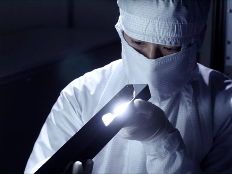
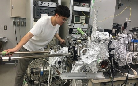
In our laboratory, basic and application studies have been carried out, regarding novel surface creation processes such as Elastic Emission Machining (EEM), Plasma Chemical Vaporization Machining (PCVM), and Catalyst Referred Etching (CARE), for flattening advanced material surfaces or fabricating ultraprecise X-ray optics. Since their process mechanisms are on chemical reaction basis, high quality surfaces with no mechanical damage can be produced. For example, targets of applications are X-ray mirror, EUV mirror, SOI wafer, and SiC/GaN substrate. By using fabricated X-ray mirrors, X-ray nanobeam systems and various X-ray microscopes has been successfully developed for various scientific fields such as biology, medical science, nanotechnology and material science.
Computational Physics Area
| Prof. | Yoshitada Morikawa |
| Assoc. Prof. | Ikutaro Hamada |
| Assis. Prof. | Yuji Hamamoto |
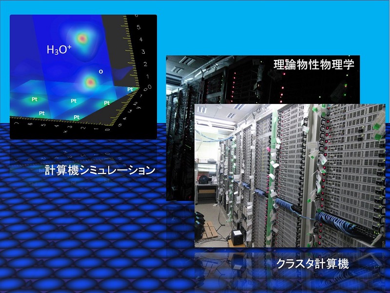
To develop highly functionalized materials for various applications such as electronic devices, solar cells, highly efficient fuel cells, organic devices, and so on,it is important to clarify behaviors of electrons and atoms in materals in detail. However, it is often difficult to elucidate such microscopic phenomena experimentally. To this end, we employ first-principles computer simulations and observe electrons and atoms in atomic scale and predict properties of new materials. We develop computer simulation programs based on ""Quantum Mechanics"" and by using those programs on super computers, we investigate physical and chemical properties of materials and clarify the origins for those properties. Based on these investigations, we propose important factors to desing new efficient materials and contribute to fields related to industry, energy and enviroment which are important in fugure of our society.
Advanced Device Engineering Area
| Prof. | Heiji Watanabe |
| Assoc. Prof. | Takuma Kobayashi |
Humanity is confronted with many global-scale issues that include depletion of fossil energy and other natural resources, food shortage and population explosion, climate change and natural disaster, and urban development and poverty. Technology has the potential for significant impact to overcome these challenges and build a sustainable society. In response to the hopes, dreams, and wishes that people find through family, friends, and community, we believe that science and technology should be developed to enable humanity to responsibly coexist and thrive with nature in environmental harmony. To realize a sustainable and prosperous future, we aim to facilitate technological innovation by designing new materials, combining dissimilar materials, and introducing new structures with wide-range of capabilities contributing to next-generation of green nanoelectronics.
nanoManufacturing Science Area
| Prof. | Kazuya Yamamura |
| Assoc. Prof. | Yuji Ohkubo |
| Assis. Prof. | Rongyan Sun |
Targets of our research center are to develop an original novel manufacturing process apparatus based on the “atomistic production engineering”, to manufacture useful “products”, and to evaluate the performance of the products.
Department of Applied Physics
Nano Physics Area
| Prof. | Yasuhiro Sugawara |
| Assis. Prof. | Yoshitaka Naitoh |
Our research focuses on novel surface and interface physics, catalytic material properties and dynamics leading to future development of nanoscience and nanotechnology employing advanced nanoprobe technology such as non-contact atomic force microscope. It covers a broad range of courses including atom/molecule manipulation, nano-phase materials, and surface nano-magnetism.
Nanomaterial Area
| Prof. | Yoshihiro Kobayashi |
| Assis. Prof. | Taiki Inoue |
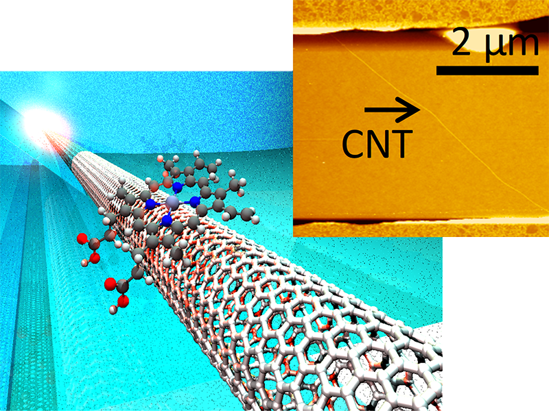
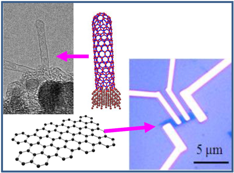
Nanomaterials, such as carbon nanotube (CNT) and graphene, have attracted considerable attention because of their unique and practically useful physical properties completely different from “bulk” materials. Our laboratory promotes the research to create novel functionalities from the nanomaterials by manipulating their structures and to apply them to future nanoelectronics. Our fabrication processes utilize originally designed apparatus such as multi-temperature zone CVD and solar furnace for ultrahigh temperature process, and are constructed by combination of top-down and self-organized bottom-up approaches, based on fundamental understanding of atomic processes on surfaces.
Nanospectroscopy Area
| Prof. | Prabhat Verma |
| Lecturer | Takayuki Umakoshi |
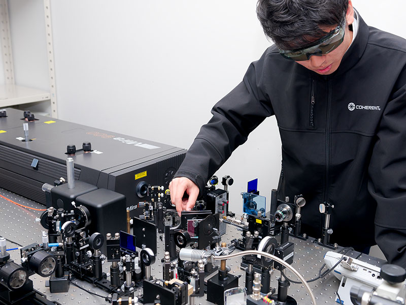
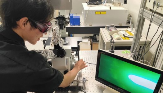
It is interesting to see nanoscale objects with light. Because the light directly interact with objects, it is possible to obtain rich information about molecular components in objects. Our group has been developing a spectroscopic technique with nanoscale spatial resolution. By combining plasmonics or near-field effect with some spectroscopic methods such as Raman scattering or photoluminescence, we can see nano-world with the visible light.
Nanophotonics Area
| Prof. | Katsumasa Fujita |
| Assis. Prof. | Yasuaki Kumamoto |
| Assis. Prof. | Stephanie Devineau |
Fujita group is creating a science and technology of “nanophotonics” - a laser technology capable of measuring, manipulating, and fabricating matters in the nano-scale world using light.
Surface Nanophysics Area
| Prof. | Kazuyuki Sakamoto |
| Assis. Prof. | Ryu Yukawa |
Our group are conducting the projects to elucidate the exotic physical properties that arise in topological quantum matters, such as atomic layer materials and topological insulators, and open a new avenue to realize next generation devices for logical operations.
Nano Biophotonics Area
| Prof. | Yasushi Inouye |
| Assoc. Prof. | Hidekazu Ishitobi |
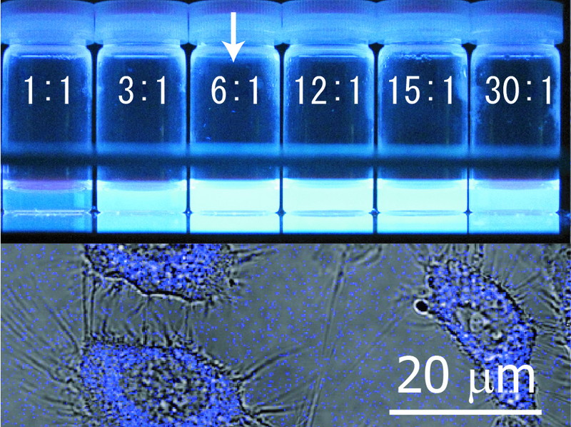
We carry out research on nano-biophotonics, a new research field that spans the fields of nanotechnology, biology, and photonics. We develop techniques to observe living cells and biomolecules with an ultra-high spatial-resolution and sensitivity by utilizing nanotechnology, vibrational spectroscopy, and non-linear photonics.
Nanoelectronics Area
| Prof. | Junichi Takahara |
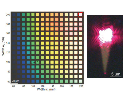
We study plasmonics (photonics of metal nanostructures) and metamaterials (optical effective media made by artificial nanostructures). For plasmonics, we investigate plasmonic waveguide, plasmonic integrated circuit, active plasmonics. For metamaterials, we investigate plasmonic metasurface as well as all-dielectric metasurface. We realize plasmonic color and all-dielectric color with diffraction limited resolution by metasurface. We realize perfect absorbers and thermal radiation IR emitters by metasurface for efficient opto-thermo conversion.
Molecular Photonics Area
| Prof. | Hiroshi Yoshikawa |
| Assis. Prof. | Takahisa Matsuzaki |
We are exploring novel materials and biological functions by using advanced optical manipulation and measurement techniques. For example, we are trying to create innovative materials (opto-electronic crystals, pharmaceutics, artificial cells, etc.) with desired structures and functions by utilizing physical stimuli of lasers (e.g., heat, electric field, etc) that enable us to control assembly and alignment of atoms/molecules. In addition, we are investigating unique structures and functions of soft matter such as biological membranes, gels, and cellular tissue (organoids) by using non-invasive optical measurement techniques that do not disturb weak attractive and/or repulsive forces in the system.
Advanced Engineering Physics Area
| Prof. | Kanta Ono |
| Assis. Prof. | Yasuo Takeichi |
Advanced Engineering Physics Area (Ono Lab.) focuses on developing advanced nano-characterization techniques using quantum beams such as X-ray and neutron beams, in combination with informatics technology to explore the structure and physical properties of materials in multiscale: from nanometer to macroscale. The goal of our research is to understand physical phenomena occurring in novel nanomaterials and nanodevices and to develop new materials and devices using these techniques.
Advanced Electron Microscope Engineering Area
| Assoc. Prof. | Yoshihide Kimura |
We are trying to figure out the phenomena occuring in a biological specimen, e.g., biological cell, DNA, chemical reactions like a catalisys, nano devices, etc. through the integration of the biology, chemistry and physics.
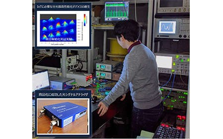
Photonic Information Technology Area
| Assoc. Prof. | Tsuyoshi Konishi |
Our group study the multidisciplinary fields that requires advanced photonic system solutions based on novel concepts for a wide range of signal processing applications including photonic networks, material and biotechnology, and so on.
Theoretical Materials Science Area
| Assoc. Prof. | Wilson Agerico Diño |
To find universality, understand the physical mechanism behind natural phenomena and the emergence of function, we conduct research and education in theoretical condensed matter physics, supported by cutting edge experimental techniques. We focus on dynamical processes and related properties at Surfaces and Interfaces of materials, size and complexity ranging from the nano-scale to biological processes. We also develop novel and practical techniques, whenever the need arises, and pro-actively make the resulting know-how available for immediate industrial implementation.
Ultimate Measurement & Nanoscience Area
| Assoc. Prof. | Yan Jun Li |
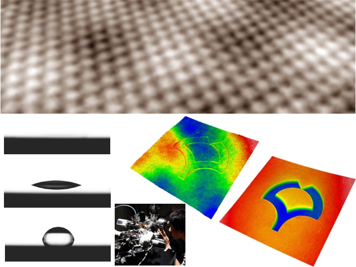
We investigate the new physical phenomena on solid surface, liquid-solid interface using the scanning probe microscopy (SPM) such as atomic force microscopy (AFM) and Kelvin probe force microscopy (KPFM) etc.
Advanced Electronic Devices Area
| Prof. | Tsuyoshi Sekitani |
| Assoc. Prof. | Kouichi Sudo |
| Assoc. Prof. | Teppei Araki |
| Assis. Prof. | Shuichi Tsuruta |
In our laboratory, we study science that fuses the basic science and advanced technologies required to precisely control the molecular structure, electronic state, and physical properties of various organic materials and to apply these technologies to realizing flexible electronics and photonics. The goals of our laboratory are to study various topics from theories based on basic science, including mathematics and physics, to systems that contribute to society.
